 TM
TM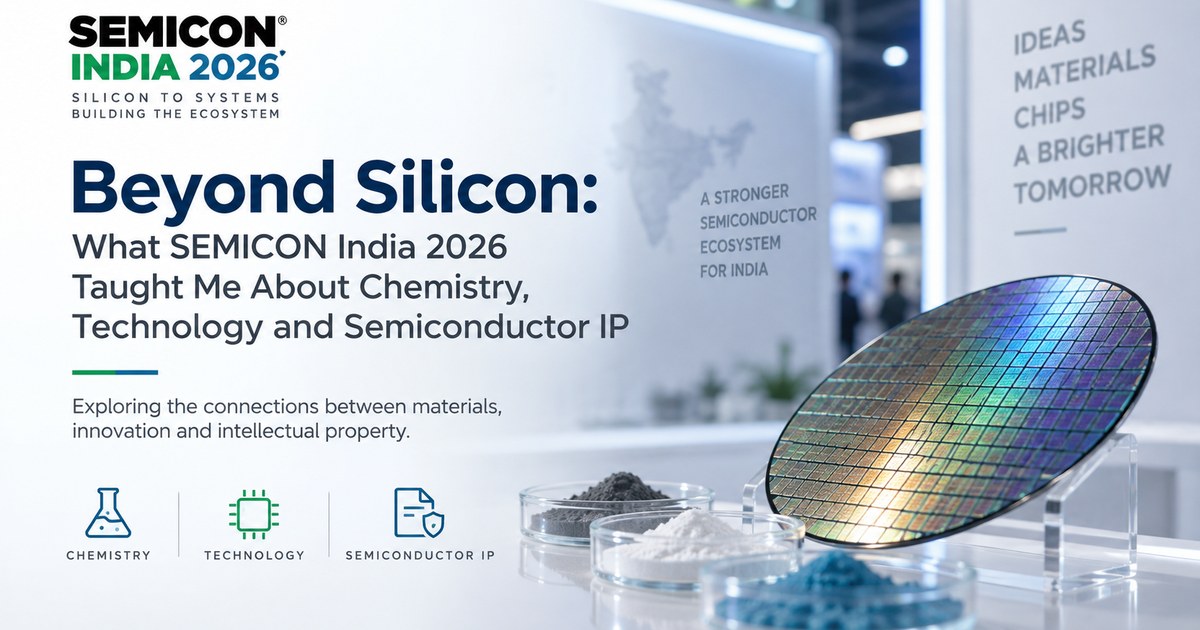
As a patent professional, I believe that keeping up with technology cannot be limited to reading patents, journals and technical literature.
“Sometimes you have to get out of the office and see the technology in action.
Hence, I visited SEMICON India 2026 at Yashobhoomi, New Delhi where participants from the entire semiconductor ecosystem met between 17 to 19 September 2026. The event's theme, “Silicon to Systems: Building the Ecosystem,” reflected the breadth of the ecosystem, from materials and manufacturing to design, startups, academia and emerging technologies.
Looking at Semiconductors through the Eyes of a Chemist
My educational background is in chemistry, and I have experience in computer applications and intellectual property, so I was particularly interested in finding out where chemistry fits into the semiconductor ecosystem.
After visiting a number of booths and talking to industry professionals, one thing stood out to me:
Semiconductor technology is more than simply silicon, electronics and chip design. It is also fundamentally a materials and chemistry-driven industry.
Chemistry and materials science are involved in numerous parts of the semiconductor value chain, from materials and deposition processes to cleaning, etching, lithography-related materials, packaging and other manufacturing processes.
The SEMICON India programme itself included a dedicated Components and Materials track, highlighting the importance of materials within the broader ecosystem.
For someone with a chemistry background, this was particularly interesting because it demonstrated how concepts that may appear highly specialised in chemistry can become critical enabling technologies in advanced electronics and semiconductor manufacturing.
Why Does This Matter to an IP Professional?
For a patent professional, understanding technology at this level is important.
Patent drafting, prosecution, prior-art analysis and claim interpretation require more than familiarity with patent law. They require an understanding of what the technology actually does, how it works and where the real technical contribution lies.
This becomes especially important in interdisciplinary technologies.
A semiconductor innovation may involve:
- materials and chemical compositions;
- semiconductor processing;
- device structures;
- manufacturing processes;
- electronic and electrical architecture;
- software and control systems;
- packaging and integration; and
- specialised equipment and process conditions.
Each of these may potentially raise different IP questions.
That makes technology mapping an important part of IP strategy.
An Interesting Interaction at IIT Indore
One of the interactions that particularly caught my attention was at the IIT Indore booth.
I got to meet with the team and look at some of the new technologies and products they’ve created.
What I found particularly encouraging was their awareness of the importance of semiconductor-related intellectual property, including areas such as semiconductor layout-design protection and IP considerations surrounding chips and processes.
For researchers and technology developers, this awareness is extremely important.
A semiconductor innovation can contain several layers of intellectual property, and identifying those layers early can help determine what should be protected, when it should be protected and through which IP mechanism.
From Technology to IP
My visit reinforced something that is easy to overlook:
An IP professional cannot remain technologically static.
Technology keeps moving, from chemistry and materials to electronics, AI, semiconductor manufacturing and advanced computing.
To provide meaningful IP support, we need to keep learning, interacting with researchers and engineers, seeing prototypes and understanding emerging technologies in the real world.
For me, SEMICON India 2026 was therefore more than an industry exhibition.
It was an opportunity to view semiconductors through the lens of chemistry, technology and intellectual property, and to see how deeply intertwined these fields are.
As India’s semiconductor ecosystem grows, I think we will see more opportunities not just for semiconductor manufacturing and chip design, but also for innovation, research and IP creation across the wider technology and materials ecosystem.
Technology evolves. IP must evolve with it.
Disclaimer: This article is intended for general educational and informational purposes only and does not constitute legal advice. The law and applicable procedures may change, and readers should seek professional advice based on their specific circumstances.